PCB Testing & Inspection
At Active-PCB Solutions, quality assurance is integrated throughout our electronics manufacturing processes. Our in-house PCB testing and inspection capabilities help identify manufacturing defects, verify assembly quality and support the demanding requirements of complex, high-reliability electronic products.
From advanced 3D Automated Optical Inspection (AOI) and X-ray inspection to flying probe and functional testing, we combine specialist equipment with experienced engineers and technicians to support consistent manufacturing standards. Our approach helps UK OEMs reduce production risks, investigate potential defects and maintain confidence in their finished assemblies.
Automated Optical Inspection (AOI) & X-Ray Inspection
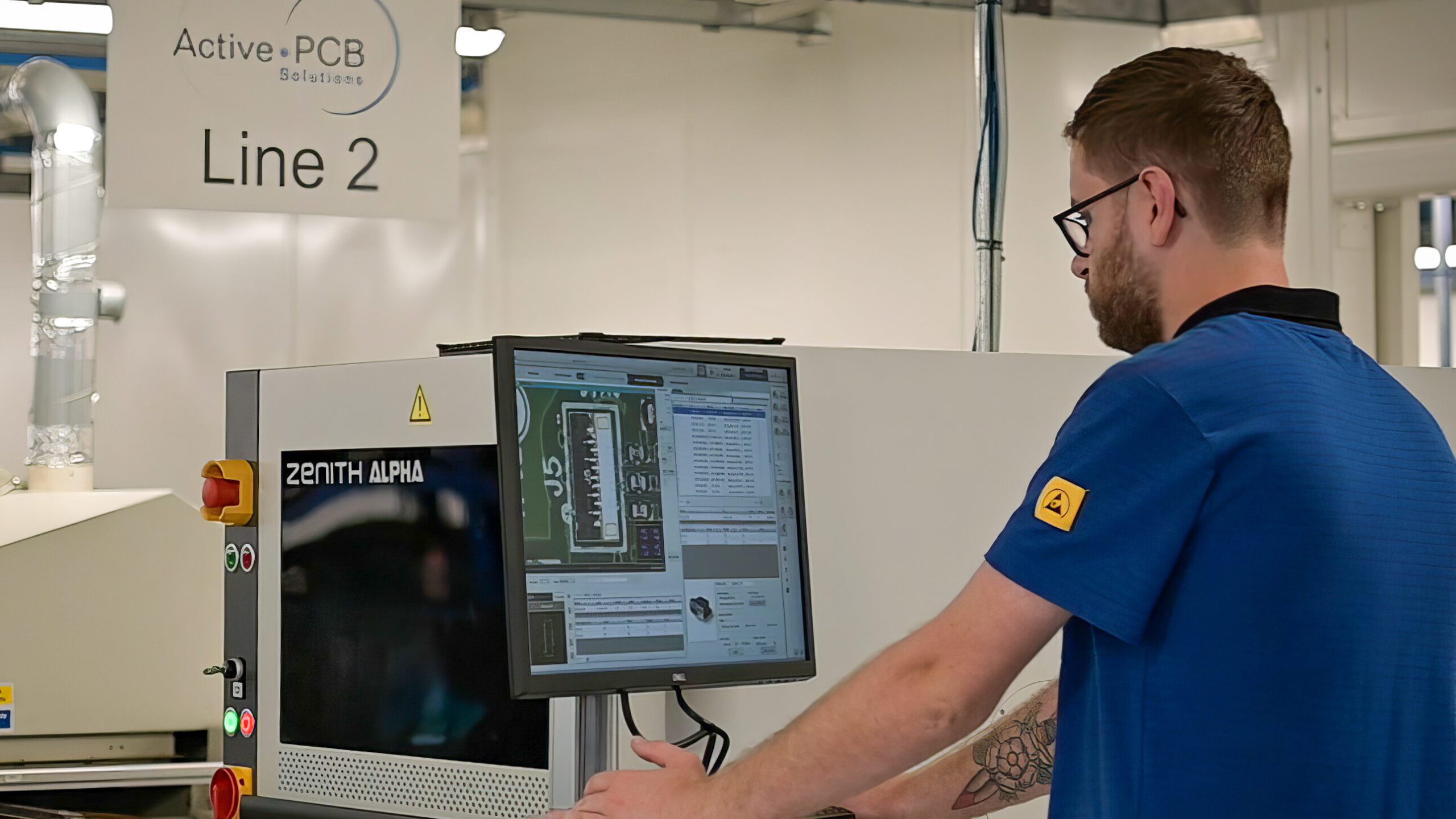
Our advanced 3D Automated Optical Inspection (AOI) and X-ray inspection equipment help identify manufacturing defects and verify PCB assemblies against specified quality requirements.
Our in-house X-ray inspection capabilities include the Nordson-Dage Quadra 3 and Nordson-Dage XD7600NT systems, allowing us to examine internal structures and solder connections that cannot be assessed through conventional visual inspection.
We also use the Koh Young Technology KSMART 3D Automated Optical Inspection (AOI) system to inspect component placement and solder joint quality. Its data collection and analysis capabilities support defect detection, process monitoring and continuous manufacturing improvement.
By combining automated inspection technologies with experienced quality personnel, we can identify potential issues during production, support corrective action and maintain consistent assembly quality.
Manual Visual Inspection
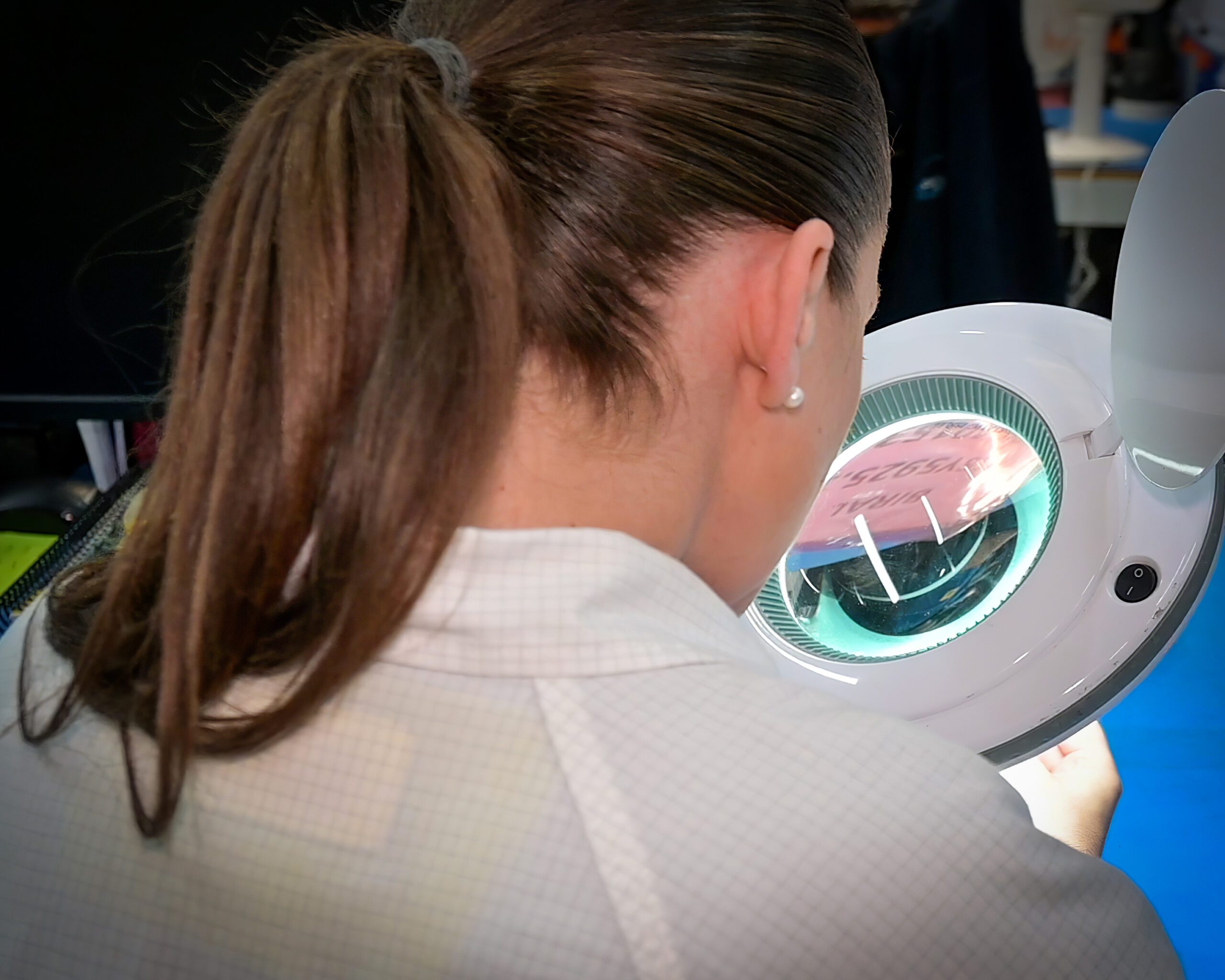
Complementing our automated processes, our IPC-A610 trained quality inspectors perform detailed visual PCB inspections using the Vision Engineering Mantis magnification system, ensuring that even the smallest components meet our high standards.
Functional PCB Testing
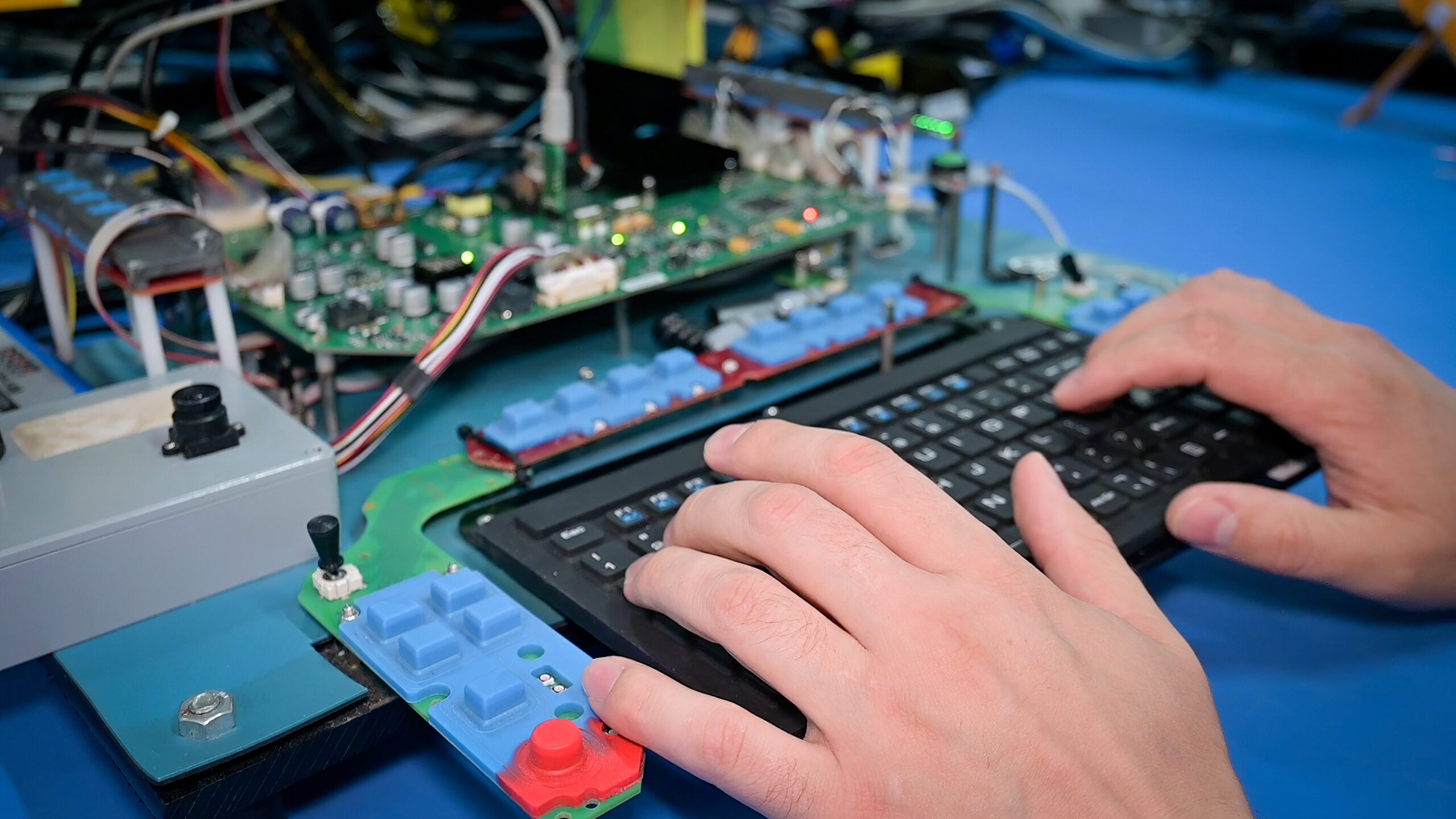
At Active-PCB Solutions, our functional PCB testing capabilities include flying probe testing, in-circuit and off-circuit programming, boundary scan, PAT and HI-POT testing. These processes help verify that electronic assemblies meet their specified electrical and functional requirements, supporting quality and reliability throughout production.
We also offer environmental stress screening to help identify potential failures by exposing assemblies to controlled conditions that simulate operational stresses. By integrating appropriate PCB testing methods into the manufacturing process, we can help identify defects before products reach customers.
Our flying probe testing capabilities provide flexible electrical testing without the need for dedicated test fixtures, making them particularly valuable for prototypes, New Product Introduction (NPI) and low-to-medium-volume PCB assembly. We also offer dedicated functional testing to verify that completed assemblies operate according to their specified requirements.